Chiplets are a way to offer continuing increases in compute capacity and I/O bandwidth needs by splitting SoC functionality into smaller heterogeneous or homogeneous dies called chiplets and integrating these chiplets into a single system in package (SIP), where the total silicon content can exceed the reticle size of a single SoC. SIP includes traditional package substrates but also may include intermediate interposers that allow higher routing density, enabling an increase in functionality and integration in a single standard or advanced package. This article delves into some of the key chiplet design and integration issues and decisions facing system designers.
System partitioning
The first question design teams need to consider is what functional blocks and functions will be included in a design and how those functions will be partitioned into different chiplets. Additionally, designers will select the semiconductor process node that is most efficient for each block. A common high-level breakdown could be compute die, IO die(s), and memory functions on different chiplets. Next is making tradeoffs related to latency, bandwidths, and power consumption that are dependent on process node selection and chiplet partitions.
Process node selection
The compute die in an AI accelerator may be ideal in the latest process node to optimize performance and power, whereas implementing cache memory in that node may not be ideal. The cache could be on the same die, but SRAM may not scale on the latest node as much as logic, so implementing SRAM on a lower cost node would be more efficient. Furthermore, latency requirements going off-chip through a 2.5D die-to-die interface will not be suitable. An option could be 3D implementation where the compute die is on latest node N and the SRAM and IO are on node N-1 or N-2. One example is the AMD Ryzen7000X3D processors with Second-Gen 3D V-Cache, integrating 3D stacked compute and SRAM memory as seen in AMD Shares New Second-Gen 3D V-Cache Chiplet Details Up to 2.5 TB/s.
For analog functions or IO interface functions like PCIe or Ethernet, there may be more tolerance for latency and can best be implemented in a separate chiplet connected by UCIe interface to the main die. The main chiplet can be on an older process node to save cost.
Die-to-die connectivity considerations
UCIe has become the de facto standard for die-to-die connectivity between chiplets, but selecting UCIe configurations requires many considerations. Designers need to understand the bandwidth requirements based on the workload of the chiplet. This may include bandwidth for the main band data but also side channel data for control and management. Using an AI server IO chiplet application as an example, UCIe bandwidth needs are related to an interface IP such as Ethernet, UALink, or PCIe.
Designers have several choices to make, including data rates for each lane and whether to use organic substrates with longer reach (UCIe standard) or use the smallest beach front and advanced packaging with smallest bump pitch (UCIe advanced). There are also tradeoffs between data rates (ranging from 16G to 64G) and how many lanes are needed to fit into die beach front constraints. The available beach front may change based on the interface IP PHY layout. Depending on the target form factor and/or aspect ratio for a chiplet, designers could select to have PHYs in a single row on a die edge. Another alternative is to double stack the PHYs in columns, so the beach front is cut in half at the expense of the PHY area depth.
Most UCIe applications make use of a streaming interface. Designers must decide on the bridge to get from UCIe streaming to the interface IP. Selections could include AXI, ARM CXS, or upcoming standards like PXS. Some considerations may be required on how to package the data into available resources without wasting bandwidth, performing clock crossing functions, and deciding whether data goes directly point-to-point from UCIe to interface IP or to an intermediate network-on-chip (NOC) to offer more flexibility on connectivity inside the chiplet.
Advanced packaging brings new capabilities and challenges
There has never been more focus on packaging technology than now. With all of these advancements come great opportunities, but also more challenges when designing an individual chiplet or chiplets for a multi-die design.
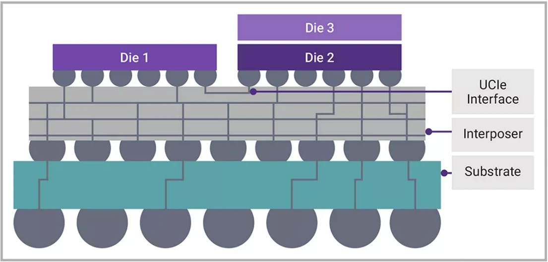
Designers need to decide how to interconnect the chiplets in a multi-die design. An organic substrate offers a lower cost and faster design schedule than a 2.5D architecture that includes interposers or interposers with silicon bridges. For more advanced use cases, intermediate interposers are likely needed to accommodate the required interconnect density and power/ground and signal paths. Once the interposer is selected, mature silicon interposers or newer organic substrate RDL interposers or RDL interposers with silicon bridges must be selected to provide denser interconnects as needed. Silicon interposers are established technologies, but are costly as they get larger and are limited in size due to brittleness. RDL interposers aim to reduce cost and offer larger sizes to integrate larger systems with more silicon content.
In all cases, designers have new challenges with mechanical form factors, signal integrity and power integrity analysis, thermal analysis of individual chiplets, but also interaction between them. There is also added complexity in bump planning and wafer probe placement to align requirements across chiplets, packaging, and test requirements. Even within a type of substrate or interposer, there could be variations in the bump pitch spacing in a typical range of 110 to 150 microns for substrates and 25-55 microns for microbumps used on interposers. There are even more variations if 3D die stacks are added, as highlighted in Figure 1.

Fig. 1: Example of 3.5D packaging with a 3D die stack connected to another 2D die via an interposer.
Another part of packaging challenges involves planning for test, including wafer probe access on chiplets to deliver known good dies (KGDs), using IEEE 1838 protocol and multi-chiplet test servers to access chips that may not be accessible from external pins directly.
Design and verification for security
IP integration presents several challenges, including issues related to interoperability, validation, and security.
Once designers have achieved a system partition amongst heterogeneous or homogeneous chiplets, there are new considerations for design security. With multi-die design, there is now a wider attack footprint to protect against. The first issue is providing attestation features to authenticate each chiplet. Then, depending on the end application, designers may need to provide a root of trust for processing sensitive data and possibly passing keys amongst systems for data encryption services. Designers can also consider secure boot processes to prevent outside tampering at hardware and firmware levels. Designers must also consider protecting data in transit across critical interfaces such as PCIe and CXL Integrity and Data Encryption (IDE), DDR and LPDDR inline memory encryption (IME), and Ethernet MACsec functions. Another option could be support for ARM Confidential Compute Architecture (CCA).
System-level simulation, emulation, and prototyping are essential steps in the development process to ensure functionality and performance to deliver first-time-right silicon. Co-design efforts should encompass silicon, software, and system components to achieve optimal integration and efficiency so designers can develop software ahead of silicon availability.
Conclusion
There are many considerations and deep experiences needed to shift from an idea to a multi-die design. Synopsys offers a broad portfolio of standards-based interface IP as well as IP subsystem integration services to deliver integration-ready chiplet subsystems. Designers can leverage Synopsys’ System Solution Design Services and ecosystem partners with advanced familiarity of Synopsys’ EDA and IP products to accelerate development and ensure optimized silicon, packaging, and software products. Designers can engage with Synopsys now to discuss their concept, architecture, IP selection, flows and methodologies, RTL, IP integration, physical implementation, package design, fab management, or collaborate with Synopsys for full end-to-end design approach. With Synopsys’ expertise and technical service, designers can focus their core competencies, while offloading other parts of the design to experts in those areas for fastest and most reliable time-to-market.
Robert Kruger
(all posts)
Robert Kruger serves as a product management director at Synopsys, where he oversees IP solutions for multi-die designs, including 2D, 3D, and 3.5D topologies. Throughout his career, he has held key roles in product marketing, business development, and roadmap planning at leading companies such as Intel, Broadcom, Nokia, and Altera. Kruger brings extensive expertise in semiconductor technologies, including ASICs and FPGA products, as well as deep knowledge of specialized requirements across various sectors, including wireless infrastructure, military, automotive, industrial, and data center markets. He holds a Bachelor of Science in Electrical Engineering (BSEE) from Boston University and a Master of Business Administration (MBA) from Santa Clara University.


