7 Powerful Reasons H100 is NVIDIA’s Best AI Accelerator
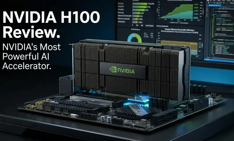
Table of Contents
H100 GPU Review: NVIDIA’s most powerful AI accelerator marks a pivotal moment in the evolution of artificial intelligence and high-performance computing (HPC). Since its official unveiling in March 2022 and subsequent launch, the NVIDIA H100 Tensor Core GPU, built on the groundbreaking Hopper architecture, has rapidly become the gold standard for accelerating the most demanding AI training and inference workloads. It is purpose-built to tackle the complexities of large language models (LLMs), generative AI, and exascale scientific simulations, delivering an unprecedented leap in computational power and efficiency over its predecessors.
Introduction: The Dawn of a New AI Era
The NVIDIA H100 GPU represents a monumental stride in accelerated computing, designed to meet the insatiable demands of an AI-driven world. At its core, the H100 is engineered to redefine the boundaries of what’s possible in deep learning and high-performance computing. Leveraging a cutting-edge TSMC 4N process, the Hopper architecture packs over 80 billion transistors, a significant increase over the previous Ampere generation. This technological marvel enables the H100 to process vast datasets and execute complex operations at speeds previously unimaginable, making it indispensable for advanced AI applications ranging from conversational AI to medical diagnosis systems and self-driving cars.
The imperative for such powerful GPUs stems from the nature of modern AI and deep learning applications, which require immense processing power for both training and inference. The H100’s architecture is meticulously optimized for these compute-intensive tasks, promising to shorten training cycles, improve inference latency, and ultimately accelerate scientific discovery. Its introduction has not only elevated performance benchmarks but has also laid the foundation for future innovations in AI, firmly establishing NVIDIA’s position at the forefront of the AI hardware revolution.
The Hopper Architecture: A Quantum Leap in AI Computing
The NVIDIA H100 is powered by the revolutionary Hopper architecture (GH100 die), named after the pioneering computer scientist Grace Hopper. This architecture introduces several groundbreaking innovations that collectively deliver an order-of-magnitude performance leap for large-scale AI and HPC.
Central to Hopper’s prowess is the Transformer Engine, a dedicated hardware component specifically designed to accelerate transformer-based models, which are fundamental to large language models (LLMs) and generative AI. The Transformer Engine dynamically adjusts precision between FP8 (8-bit floating-point) and FP16 (16-bit floating-point) formats, intelligently selecting the optimal precision to maximize throughput without compromising model accuracy. This dynamic precision scaling can deliver up to 4-9x faster performance compared to the A100 for training large transformers like GPT and LLaMA models.
Another significant advancement is the integration of Fourth-Generation Tensor Cores. These specialized cores are up to 6x faster chip-to-chip compared to the A100, providing enhanced computational rates on various data types, including FP8. They accelerate a broad array of AI and HPC tasks, tripling the floating-point operations per second (FLOPS) for TF32, FP64, FP16, and INT8 precisions over the prior generation.
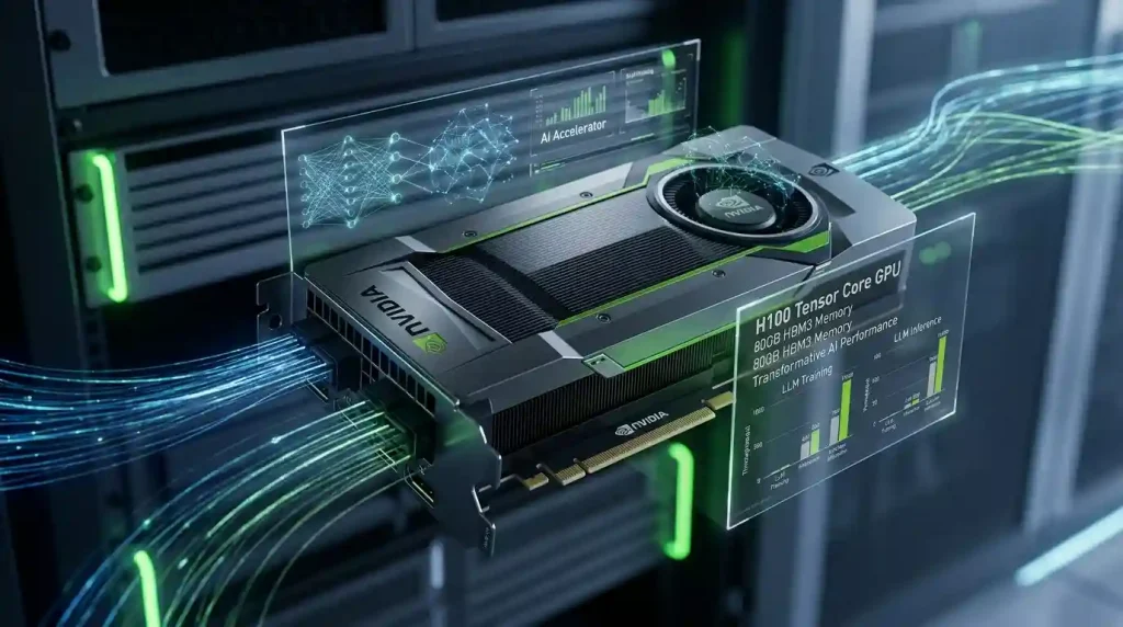
Hopper also features a vastly improved memory subsystem. The H100 SXM variant is equipped with 80GB of HBM3 memory, boasting an impressive 3.35 TB/s of memory bandwidth. This represents a roughly 67% increase over the A100’s 2 TB/s HBM2e memory, effectively removing memory bottlenecks that often limit the performance of memory-bound inference workloads, especially for large models. The PCIe variant of the H100 also offers 80GB of memory, though it uses HBM2e with ~2 TB/s bandwidth.
For multi-GPU scaling, the H100 incorporates NVLink Gen4, providing 900 GB/s of bidirectional interconnect bandwidth per GPU. This enables near-linear efficiency in scaling across multiple GPUs, allowing for the creation of massive, unified GPU clusters capable of handling exascale workloads. The NVLink Switch System further enhances communication across nodes, crucial for training trillion-parameter AI models. Additionally, the H100 supports PCIe Gen5, offering 128GB/s of bandwidth for connectivity to the rest of the system.
The Hopper architecture also introduces NVIDIA Confidential Computing, the world’s first accelerated computing platform with hardware-based confidential computing capabilities. This feature protects data and models during processing, ensuring confidentiality and integrity for regulated industries such as healthcare, finance, and government.
Learn more about the fundamentals of GPU acceleration.
Key Specifications and Unmatched Performance Metrics
The NVIDIA H100 GPU’s specifications underscore its dominance in the AI accelerator market. Available in both SXM5 and PCIe form factors, the SXM5 variant generally offers higher performance due to its superior power delivery and NVLink capabilities.
Here’s a snapshot of the H100 SXM5’s key specifications:
- CUDA Cores: 16,896
- Tensor Cores: 528 (4th Generation) with FP8 Transformer Engine
- GPU Memory: 80GB HBM3
- Memory Bandwidth: 3.35 TB/s
- FP8 Throughput: Up to 3,958 TFLOPS (with sparsity)
- TF32 Throughput: 989 TFLOPS (with sparsity)
- FP64 Throughput: 60 TFLOPS
- TDP (Thermal Design Power): 700W
- NVLink: NVLink 4.0, 900 GB/s bidirectional bandwidth per GPU
- Multi-Instance GPU (MIG): Up to 7 isolated GPU instances
- Form Factor: SXM5 (requires compatible server platforms like DGX H100, HGX H100)
The PCIe variant, while still highly capable, presents slightly different figures: 14,592 CUDA cores, 456 Tensor Cores, and 80GB HBM2e memory with ~2 TB/s bandwidth, and a TDP of 350W. It supports PCIe Gen5 but generally lacks full NVLink support, instead relying on NVLink bridges for intra-node scaling.
In terms of raw performance, the H100 delivers exceptional FLOPS performance across various precisions. It boasts a theoretical peak performance exceeding 1 ExaFLOP of AI compute power using FP8 precision, making it suitable for the most demanding AI workloads. This incredible computational density, combined with its high memory bandwidth, makes the H100 a formidable accelerator for both AI training and inference.
H100 vs. A100: A Generational Shift
The NVIDIA H100 is designed as a direct successor to the A100, built on the Ampere architecture. The generational leap is profound, addressing the escalating demands of contemporary AI workloads, particularly those involving large language models.
Here’s a comparative analysis highlighting the key differences:
| Feature | NVIDIA H100 (SXM) | NVIDIA A100 (SXM) | Significance |
|---|---|---|---|
| Architecture | Hopper (GH100) | Ampere (GA100) | New architecture optimized for transformer-based AI. |
| Transistors | 80 billion | 54.2 billion | Increased density for more compute power. |
| Manufacturing Process | TSMC 4N | TSMC 7nm | More efficient and powerful chip. |
| Tensor Cores | 4th Gen with FP8 Transformer Engine | 3rd Gen | Dedicated engine for LLMs, FP8 precision. |
| GPU Memory | 80GB HBM3 | 40GB or 80GB HBM2e | Larger capacity and faster memory type. |
| Memory Bandwidth | 3.35 TB/s | 2.0 TB/s | 67% faster, crucial for memory-bound tasks. |
| NVLink Bandwidth | 900 GB/s (Gen4) | 600 GB/s (Gen3) | 50% higher, improving multi-GPU scaling. |
| FP8 Throughput | 3,958 TFLOPS | Not supported | Significant acceleration for transformer models. |
| AI Training Speed | Up to 4x faster (GPT-3 175B) | Baseline | Dramatic reduction in training times for large models. |
| AI Inference Speed | 1.5-2x faster (LLMs) | Baseline | Faster token generation and lower latency. |
| Max TDP | 700W | 400W | Higher power for increased compute capacity. |
| Confidential Computing | Hardware-based TEE | Limited/None | Enhanced data security for sensitive workloads. |
Benchmarks consistently show the H100 delivering a substantial performance lead. For mixed-precision training, the H100 offers up to 2.4 times faster throughput than the A100, with even greater improvements for very large models. In large language model inference, the H100 can generate 250 to 300 tokens per second, compared to the A100’s around 130 tokens per second for similar models. While the A100 remains a capable GPU, especially for cost-sensitive deployments or a variety of AI models, the H100 is the clear choice for cutting-edge performance in transformer-heavy, data-intensive workloads, offering “future-proofing” for AI infrastructure.
Unleashing AI Capabilities: Target Applications and Use Cases
The NVIDIA H100 GPU is not just a powerful chip; it’s an accelerator designed to transform various facets of AI and HPC. Its architectural innovations specifically target areas where traditional GPUs hit performance bottlenecks.
Large Language Models (LLMs) and Generative AI: This is arguably where the H100 shines brightest. The Transformer Engine and FP8 precision are tailor-made for the massive computational demands of training and inferencing LLMs like GPT-3, LLaMA 2-70B, and other generative AI models. It can accelerate LLM training by up to 30 times and inference by up to 30 times over the A100, enabling the development of more sophisticated conversational AI, recommender systems, and code generation tools.
High-Performance Computing (HPC): The H100 significantly boosts HPC capabilities, tripling the FP64 (double-precision) Tensor Core FLOPS to deliver 60 teraFLOPS for scientific simulations. This empowers researchers to accelerate complex computations in areas like climate modeling, genomics, drug discovery, and financial risk analysis. Its ability to handle AI-fused HPC applications with TF32 precision, achieving one petaFLOP of throughput, means scientists can accelerate time to discovery with minimal code changes.
Data Analytics: Large datasets are a common challenge in AI application development. The H100, with its 3 TB/s memory bandwidth and scalability with NVLink and NVSwitch, provides the compute power to accelerate data analytics workloads, enabling high performance and supporting massive datasets. This is critical for tasks where the majority of time is spent on data preparation and processing.
Real-Time Deep Learning Inference: The H100 excels in production LLM inference at scale, offering optimal latency and throughput for medium-to-large batch sizes. Its 80GB HBM3 VRAM allows for serving large models (30B-70B+ parameters) at full precision without extensive quantization, crucial for real-time applications such as chatbots, fraud detection, and image/speech recognition. The H100’s Multi-Instance GPU (MIG) feature also supports multi-tenant inference by partitioning the GPU into up to seven isolated instances, ensuring consistent Quality of Service (QoS).
Enterprise AI and Secure Workloads: With hardware-based confidential computing (TEE), the H100 ensures data and model integrity and privacy during processing. This makes it an ideal solution for compliant AI deployments in highly regulated sectors, offering robust security features necessary for enterprise-grade applications.
Explore other AI solutions for enterprise infrastructure.
The Robust Software Ecosystem and Developer Support
NVIDIA’s dominance in the AI hardware market is significantly bolstered by its comprehensive software ecosystem, with CUDA (Compute Unified Device Architecture) at its heart. CUDA is NVIDIA’s parallel computing platform, acting as the bridge between the powerful H100 hardware and the myriad of AI and HPC applications.
The H100 GPU is designed to seamlessly integrate with the existing CUDA ecosystem, meaning developers can leverage their familiar tools and libraries to harness its immense power. This includes popular deep learning frameworks like TensorFlow and PyTorch, which are optimized to utilize GPU acceleration via CUDA. The stability and maturity of CUDA, developed over nearly two decades, represent a significant competitive moat for NVIDIA, as switching to alternative platforms often requires extensive code rewriting and performance trade-offs.
Beyond CUDA, NVIDIA provides a rich suite of software components that further enhance the H100’s capabilities:
- NVIDIA AI Enterprise: This software suite acts as the operating system for the NVIDIA AI platform, offering a comprehensive collection of AI frameworks, libraries, and tools optimized for production-ready AI applications. It includes solutions for speech AI, recommenders, chatbots, cybersecurity, and more, ensuring that organizations can deploy and manage their AI workloads efficiently on H100 infrastructure.
- NVIDIA Magnum IO: This software stack optimizes data movement and communication within large GPU clusters, ensuring efficient scalability for demanding workloads across multiple nodes.
- NVIDIA Quantum-2 InfiniBand: Critical for high-speed GPU-to-GPU and node-to-node communication in data centers, this networking technology minimizes latency and maximizes throughput, essential for large-scale distributed training.
- NVIDIA RAPIDS™: A suite of software libraries for accelerating data science pipelines, enabling faster processing of massive datasets on H100 GPUs.
The combination of the H100’s cutting-edge hardware with NVIDIA’s robust and deeply integrated software stack creates an unparalleled platform for AI and HPC development, making it the de facto standard for researchers and enterprises pushing the boundaries of what’s possible in AI.
Challenges, Costs, and Future Outlook
While the NVIDIA H100 GPU represents a pinnacle of AI acceleration, its deployment comes with certain challenges and considerations, particularly regarding cost, power consumption, and availability.
Cost: The H100 is a premium product, reflecting its advanced technology and performance. The direct purchase cost for an individual H100 GPU can start around $25,000, with high-end configurations like the H100 80GB reaching over $30,000. For multi-GPU systems, costs can quickly escalate, with an 8-GPU server potentially exceeding $400,000. Beyond the GPUs themselves, significant infrastructure expenses are involved, including high-speed InfiniBand networking, specialized power distribution units, and advanced cooling systems, which can add tens to hundreds of thousands of dollars to the total setup cost.
Power Consumption and Cooling: The H100 SXM variant has a Thermal Design Power (TDP) of 700W, nearly double that of the A100. While this higher power fuels its immense compute capacity, it necessitates robust power infrastructure and advanced cooling solutions, making it unsuitable for typical personal workspaces. Data centers deploying H100 clusters must account for substantial energy loads and efficient heat dissipation to ensure optimal performance and operational stability.
Availability and Supply Chain: Despite being available since 2022, the demand for H100 GPUs has consistently outstripped supply, leading to significant wait times and upward pressure on rental prices. Since late 2025, H100 rental prices have surged by nearly 40% in some instances, even with the introduction of newer architectures like Blackwell. This “great GPU shortage” is exacerbated by persistent supply chain bottlenecks, particularly concerning High Bandwidth Memory (HBM3) and advanced CoWoS packaging technologies. These constraints indicate a systemic lack of AI computing power across the board, affecting both older and newer generation chips. The imbalance between supply and demand underscores NVIDIA’s pricing power in a market desperate for its technology.
For many organizations, especially those without sustained, predictable workloads, renting H100 GPUs through cloud providers often proves more cost-effective than outright purchasing. Rental costs typically range from $2.00 to $10.00 per GPU-hour, allowing for immediate access and avoiding large upfront capital expenditures and ongoing operational overhead. Buying only becomes economically viable for teams running sustained workloads exceeding 10,000 GPU-hours monthly for multiple years.
Looking ahead, the H100’s impact will continue to shape the AI landscape for years to come. While newer GPUs like the H200 (with increased memory capacity and bandwidth) and the Blackwell series (B200/GB200) are emerging, the H100 remains a cornerstone of current AI infrastructure, defining the performance baseline for production AI in 2026. Its continued relevance highlights the rapid innovation and intense demand characterizing the AI hardware market, pushing the boundaries of what machines can achieve. Further insights into the broader context of semiconductor supply chain challenges can be found on Wikipedia’s page on the Semiconductor Industry.
Conclusion: Charting the Future of AI
The NVIDIA H100 GPU stands as a testament to engineering excellence, solidifying NVIDIA’s position as the uncontested leader in AI acceleration. Through its Hopper architecture, featuring innovations like the Transformer Engine, fourth-generation Tensor Cores, HBM3 memory, and NVLink Gen4, the H100 delivers unprecedented performance gains, particularly for large language models and high-performance computing. It has redefined the benchmarks for AI training and inference, enabling researchers and enterprises to tackle previously insurmountable computational challenges.
While the H100’s premium cost, significant power requirements, and ongoing supply chain challenges necessitate careful planning and investment, its benefits in accelerating AI development and deployment are undeniable. For organizations aiming to push the boundaries of generative AI, scientific discovery, and real-time data analytics, the H100 is not merely an upgrade; it is a fundamental enabler of future innovation. As the AI landscape continues its rapid expansion, the H100 will undoubtedly remain a critical component, driving advancements that will shape the technological world for years to come.