GPU A100 Review: NVIDIA’s AI Powerhouse for Deep Learning – 10 Key Performance Insights

Table of Contents
GPU A100 has irrevocably transformed the landscape of artificial intelligence and high-performance computing (HPC) since its unveiling in May 2020. As the flagship product of NVIDIA’s data center platform, this Tensor Core GPU, built upon the revolutionary Ampere architecture, heralded an unprecedented era of acceleration for demanding computational workloads. Designed from the ground up to unify AI training and inference, alongside data analytics and scientific computing, the A100 offers a performance leap of up to 20 times over its predecessor, the NVIDIA Volta generation. This remarkable advancement has positioned the A100 as a cornerstone for modern data centers, cloud service providers, and research institutions striving to push the boundaries of innovation.
The NVIDIA A100 is not merely an incremental upgrade; it represents a significant architectural shift that redefines what is possible in accelerated computing. Its introduction marked a pivotal moment, enabling researchers and developers to tackle increasingly complex AI models and simulations that were previously infeasible. From accelerating massive language models like GPT-3 to powering sophisticated scientific simulations, the A100’s versatility and raw computational power have made it an indispensable tool for engineers and scientists worldwide. This comprehensive review delves into the core technologies, specifications, performance metrics, and real-world applications that solidify the NVIDIA A100’s reputation as a true AI powerhouse.
The Ampere Architecture: Foundation of GPU A100
At the heart of the NVIDIA A100 lies the groundbreaking Ampere architecture, a testament to NVIDIA’s engineering prowess. Officially announced on May 14, 2020, and named after the French mathematician and physicist André-Marie Ampère, this microarchitecture succeeded both the Volta and Turing architectures, bringing forth a new era of GPU design. The A100 GPU itself is based on the GA100 chip, which is manufactured using TSMC’s 7-nanometer FinFET process and incorporates a staggering 54 billion transistors, making it one of the largest 7-nanometer processors ever created.
The Ampere architecture introduces several critical improvements that are fundamental to the A100’s unparalleled performance. One of the most significant innovations is the third-generation Tensor Cores, which are far more flexible and powerful than previous generations. These specialized AI math units are designed to dramatically boost deep learning performance, offering support for a broad range of math precisions including FP16, BFloat16 (BF16), TensorFloat-32 (TF32), and even FP64 for high-performance computing applications. Specifically, TF32 provides up to 20 times higher AI compute over FP32 precision with zero code changes, simplifying the adoption of accelerated computing for many AI workloads.
Beyond the Tensor Cores, the Ampere architecture also introduced enhanced streaming multiprocessors (SMs). The A100 incorporates 108 SMs, each equipped with 64 FP32 CUDA Cores, contributing to its formidable processing power. This design optimizes the GPU for diverse computational tasks, from general-purpose computing to complex machine learning operations. The architectural enhancements also extend to asynchronous copy and barrier technologies, which enable more efficient data transfer and synchronization between computing tasks, reducing power consumption and enhancing overall performance in large multi-GPU clusters.
Key Features and Innovations Driving Performance
The NVIDIA A100 distinguishes itself through a suite of innovative features designed to maximize performance, efficiency, and versatility for AI and HPC workloads:
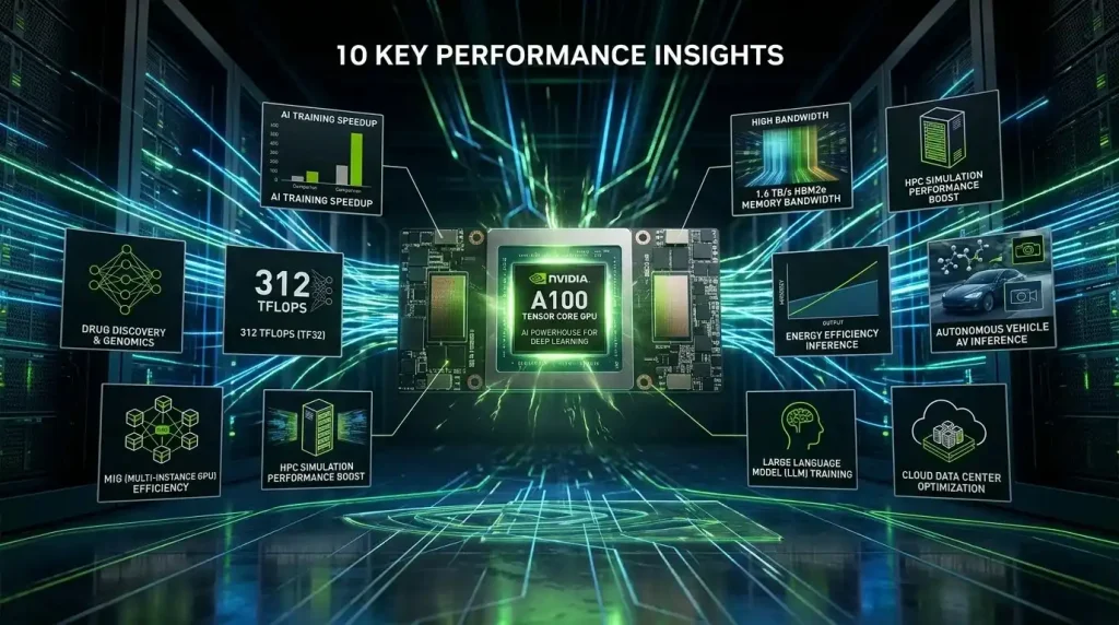
- Third-Generation Tensor Cores: As highlighted, these cores are the backbone of the A100’s AI capabilities. They provide a 20x performance boost over previous generations for deep learning workloads. They support a full range of precision from FP32 to INT4 and introduce Tensor Float 32 (TF32) for AI training and FP64 Tensor Core operations for HPC, delivering a significant leap in throughput across various numerical formats.
- Multi-Instance GPU (MIG) Technology: A game-changer for resource utilization, MIG allows a single A100 GPU to be partitioned into up to seven fully isolated GPU instances. Each instance comes with its own high-bandwidth memory, cache, and compute cores, providing guaranteed quality of service (QoS) for various workloads. This is particularly beneficial in cloud environments and research labs, enabling multiple users or applications to run concurrently without interference, maximizing GPU utilization.
- Next-Generation NVLink and NVSwitch: The A100 features NVLink 3.0, which doubles the high-speed connectivity between GPUs compared to the previous generation, achieving an impressive 600 GB/s of interconnect bandwidth. When combined with NVIDIA NVSwitch, up to 16 A100 GPUs can be interconnected, unleashing the highest application performance possible on a single server and enabling seamless GPU scaling for large models.
- High-Bandwidth Memory (HBM2e): The A100 comes in 40GB and 80GB variants of HBM2e memory. The 80GB model boasts the world’s fastest GPU memory bandwidth at over 2 terabytes per second (TB/s), while the 40GB model offers 1.6 TB/s. This massive memory capacity and bandwidth are crucial for handling colossal datasets and training giant neural networks that can easily consume tens of gigabytes for model parameters and activations.
- Structural Sparsity: This innovative feature leverages the inherently sparse nature of AI math to deliver up to 2x higher performance for sparse models during both training and inference. Many neural networks have redundant parameters that can be converted to zeros without compromising accuracy, and the A100’s Tensor Cores can efficiently process these sparse models.
- PCIe Gen4 Support: The A100 supports PCIe Gen4, offering twice the bandwidth of PCIe Gen3, which significantly improves CPU-to-GPU communication and overall data transfer speeds, crucial for data-intensive workloads.
A Deep Dive into Technical Specifications
Understanding the raw specifications of the NVIDIA A100 reveals the meticulous engineering behind its performance:
The A100 is based on the Ampere GA100 GPU, fabricated on a 7nm process. It packs 6,912 CUDA Cores for general-purpose parallel processing and 432 third-generation Tensor Cores dedicated to accelerating AI workloads. For specific numerical precisions, the A100 delivers:
- FP64 Performance: Up to 9.7 TFLOPS (double-precision). With FP64 Tensor Cores, it can reach 19.5 TFLOPS, a significant boost for HPC simulations.
- FP32 Performance: Up to 19.5 TFLOPS (single-precision).
- Tensor Float 32 (TF32): Up to 156 TFLOPS, with structural sparsity enabled, this can reach 312 TFLOPS. This is a key accelerator for AI training.
- FP16/BFloat16 Tensor Core Performance: Up to 312 TFLOPS, and up to 624 TFLOPS with structural sparsity.
- INT8 Tensor Core Performance: Up to 624 TOPS, and up to 1248 TOPS with structural sparsity, ideal for highly optimized AI inference.
Memory configurations are another crucial aspect. The A100 is available with either 40GB of HBM2 or 80GB of HBM2e (High-Bandwidth Memory 2 extended). The 40GB model offers a memory bandwidth of 1.6 TB/s, while the 80GB variant reaches an impressive 2.0 TB/s. This enormous memory bandwidth and capacity are vital for training large language models and handling data-intensive HPC tasks. The A100 also features a substantial 40 MB of L2 cache to further enhance data access efficiency.
In terms of power, the A100 PCIe 40GB has a maximum thermal design power (TDP) of 250W, while the 80GB PCIe version draws up to 300W. The SXM form factors can go up to 400W. These power envelopes necessitate robust cooling solutions, typically passive cooling, designed for integration into server chassis with engineered airflow.
| Feature | NVIDIA A100 40GB (PCIe) | NVIDIA A100 80GB (PCIe) |
|---|---|---|
| Architecture | Ampere (GA100, 7nm) | Ampere (GA100, 7nm) |
| CUDA Cores | 6,912 | 6,912 |
| Tensor Cores (3rd Gen) | 432 | 432 |
| GPU Memory | 40GB HBM2 | 80GB HBM2e |
| Memory Bandwidth | 1.6 TB/s (1555 GB/s) | 2.0 TB/s (2039 GB/s) |
| FP32 Performance | 19.5 TFLOPS | 19.5 TFLOPS |
| TF32 Tensor Core Performance (with sparsity) | 312 TFLOPS | 312 TFLOPS |
| MIG Support | Up to 7 instances @ 5GB | Up to 7 instances @ 10GB |
| NVLink Bandwidth | 600 GB/s (with NVLink Bridge for 2 GPUs) | 600 GB/s (with NVLink) |
| PCIe Interface | PCIe Gen4 x16 | PCIe Gen4 x16 |
| Max TDP | 250 W | 300 W |
Unleashing Raw Power: Performance Benchmarks
The true measure of a GPU’s capability lies in its real-world performance benchmarks, and the NVIDIA A100 consistently delivers exceptional results across various AI and HPC workloads. NVIDIA claims the A100 offers up to 20 times higher performance than its predecessor, the V100, a claim largely substantiated by independent testing.
For deep learning training, the A100 showcases significant speedups. In a study comparing A100 with V100 clusters, convolutional neural network (CNN) training was approximately 55% faster on the A100, while language model training saw an impressive ~170% speedup. Benchmarks have demonstrated that the A100 achieves a 2.2x speed-up for convnets and 3.4x for transformers when using 32-bit precision, with even greater gains observed in mixed-precision training. The A100’s Tensor Cores with TF32 provide up to 20x higher performance over NVIDIA Volta with zero code changes, and an additional 2x boost with automatic mixed precision and FP16.
Deep learning inference also sees substantial acceleration. The A100 accelerates inference throughput up to 249x over CPUs on state-of-the-art conversational AI models like BERT. For the most complex, batch-size-constrained models, the A100 80GB’s increased memory capacity doubles the size of each MIG instance, leading to up to 1.25x higher throughput. Its ability to handle a full range of precision, from FP32 to INT4, further optimizes inference workloads.
In the realm of high-performance computing, the A100 introduces double-precision Tensor Cores, representing the biggest leap in HPC performance since the introduction of GPUs for these tasks. Researchers can reduce a 10-hour, double-precision simulation to under four hours on an A100. HPC applications can also leverage TF32 to achieve up to 11x higher throughput for single-precision dense matrix-multiply operations. For applications with massive datasets, the A100 80GB’s additional memory delivers up to a 2x throughput increase in simulations like Quantum Espresso.
The A100 has also set multiple performance records in MLPerf, the industry-wide benchmark for AI training, demonstrating its leadership in the field. For instance, a training workload like BERT can be solved at scale in under a minute using 2,048 A100 GPUs, a world record for time to solution.
Revolutionizing Industries: A100’s Impactful Use Cases
The versatility and raw power of the NVIDIA A100 have led to its adoption across a multitude of industries, driving breakthroughs and accelerating workflows:
- Artificial Intelligence R&D: The A100 is a cornerstone for developing and training cutting-edge AI models, including large language models (LLMs) and generative AI. Meta utilized 16,000 NVIDIA A100 GPUs to train its Llama and Llama 2 models, processing terabytes of data to generate human-like responses. Its high memory bandwidth and TF32 support make it ideal for handling GPT-3 sized models and multimodal AI.
- High-Performance Computing (HPC): For scientific research, simulations, and complex analyses, the A100 provides unmatched acceleration. Shell, an international energy company, deployed A100 GPUs for HPC to process and analyze vast amounts of data in oil and gas exploration, improving computational efficiency in seismic imaging and reservoir simulation. Similarly, it’s used in molecular dynamics, physics, engineering, and climate modeling.
- Data Analytics and Business Intelligence: The A100 propels data analytics by providing ready-to-run, optimized AI software, enabling data scientists to make sense of enormous structured and unstructured datasets. It accelerates data processing and analysis, providing rapid insights for critical business applications.
- Healthcare and Drug Discovery: In healthcare, the A100 transforms medical imaging by enhancing diagnostic accuracy and reducing processing time. During the COVID-19 pandemic, Caption Health leveraged A100 to develop AI models for echocardiography. In the pharmaceutical sector, it accelerates drug discovery by enabling simulations of complex biological systems and rapid analysis of genetic data.
- Financial Forecasting and Fraud Detection: The A100’s ability to handle massive datasets and perform real-time predictions makes it invaluable for complex financial models, algorithmic trading, and robust fraud detection systems.
- Deep Video Analytics: From media publishers to surveillance systems, the A100’s capacity for high-speed data transmission is perfect for image recognition, contactless attendance, and extracting actionable insights from streaming video clips.
The NVIDIA Software Ecosystem: Amplifying A100’s Potential
A hardware powerhouse like the A100 would be significantly limited without a robust and comprehensive software ecosystem to support it. NVIDIA has cultivated an extensive software stack that amplifies the A100’s capabilities, making it accessible and efficient for developers and researchers. This ecosystem has evolved over 15+ years, providing tools for every step of the AI and HPC software lifecycle.
Central to this ecosystem is CUDA (Compute Unified Device Architecture), NVIDIA’s parallel computing platform and programming model. CUDA allows developers to utilize various high-level programming languages, including C, C++, Fortran, and Python, to program GPUs effectively. This broad language support ensures that a wide array of existing applications can be ported and optimized for A100. The NVIDIA HPC SDK is a comprehensive package that provides compilers for C, C++, and Fortran, math and communication libraries, and performance analysis tools for developing applications on the NVIDIA platform.
The NVIDIA NGC catalog is another critical component, offering a hub of GPU-optimized software, including deep learning frameworks, HPC applications, and pre-trained AI models. These containers are tested, maintained, and optimized by NVIDIA, simplifying deployment and ensuring peak performance. This greatly reduces the setup time and complexity for businesses and researchers, allowing them to focus on innovation rather than infrastructure. Key frameworks like TensorFlow, PyTorch, and MXNet are readily available and optimized for the A100, enabling seamless integration into existing workflows.
Additionally, NVIDIA works closely with ecosystem partners to provide scheduling and orchestration tools, cluster management, and monitoring utilities, facilitating the deployment and management of A100-powered infrastructure in data centers and cloud environments. Technologies like NVIDIA Magnum IO SDK further enable scaling to thousands of A100 GPUs, allowing for world-record time-to-solution for large training workloads.
A100 vs. H100: A Brief Comparison and Future Outlook
While the NVIDIA A100 remains an extraordinary powerhouse, NVIDIA introduced its successor, the H100, based on the Hopper architecture, in 2022. The comparison between these two GPUs highlights the relentless pace of innovation in the AI hardware space and provides context for the A100’s position in the current market.
The H100 significantly builds upon the A100’s capabilities, particularly for large-scale AI, especially transformer and large language model (LLM) workloads. Key differences include:
- Architecture: A100 uses Ampere, H100 uses Hopper.
- Manufacturing Process: A100 is 7nm, H100 is 5nm.
- CUDA Cores & Tensor Cores: The H100 has a substantial increase, featuring 16,896 CUDA cores and 528 Tensor Cores compared to the A100’s 6,912 CUDA cores and 432 Tensor Cores.
- Memory: While both typically offer 80GB, the H100 uses faster HBM3 memory (up to 3.35 TB/s) compared to the A100’s HBM2e (up to 2.0 TB/s).
- Performance: The H100 delivers notable speedups, with NVIDIA reporting up to 30x faster AI inference and up to 4x faster training for massive models like GPT-3 compared to the A100. Independent tests show 2-3x gains for training and 10-20x for inference in many cases. This is driven by fourth-generation Tensor Cores and new FP8 precision with the Transformer Engine in the H100.
- Power Consumption: The H100 generally consumes more power (up to 700W) compared to the A100 (up to 400W for SXM, 300W for PCIe), but often offers better performance-per-watt for demanding AI models due to its efficiency gains.
Despite the emergence of the H100, the A100 remains a highly relevant and powerful GPU. It strikes an excellent balance between performance and cost-efficiency, making it a strong contender for a wide variety of AI and HPC workloads. It is still widely available in cloud platforms and GPU marketplaces. For teams on a budget or those with workloads optimized for FP32/FP16 precision, the A100 offers robust capabilities, high memory capacity, and proven performance, especially for batch inference, image processing, multi-tenant training, and hosting LLMs under ~16B parameters. Its Multi-Instance GPU (MIG) technology continues to be a significant advantage for optimizing utilization in multi-tenant environments.
The market for A100 GPUs remains active, with prices for refurbished 40GB units starting around $7,800 and 80GB PCIe cards around $18,900 as of early 2026. This reflects its continued demand and utility in the evolving landscape of AI infrastructure.
For more detailed information on NVIDIA’s Ampere architecture, you can refer to its Wikipedia page.
Conclusion: The Enduring Legacy of the A100
The NVIDIA A100 Tensor Core GPU has firmly established itself as a foundational technology in the accelerated computing era. Its groundbreaking Ampere architecture, coupled with innovations like third-generation Tensor Cores, Multi-Instance GPU (MIG) technology, and high-bandwidth memory, delivered an unprecedented leap in performance for AI, HPC, and data analytics. From revolutionizing scientific discovery and drug research to powering the most advanced AI models and intricate financial simulations, the A100 has provided the raw compute power necessary to tackle some of the world’s most complex computational challenges.
While newer generations like the H100 push the absolute performance envelope further, the A100 maintains its relevance as a cost-effective, versatile, and highly capable accelerator. Its widespread adoption in cloud environments and data centers, coupled with a mature and expansive software ecosystem, ensures its continued utility for a broad spectrum of applications. The A100’s legacy is not just about raw speed; it’s about making advanced AI and HPC more accessible and efficient, democratizing accelerated computing, and enabling countless innovations that continue to shape our technological future.